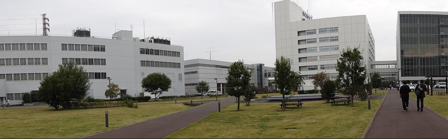
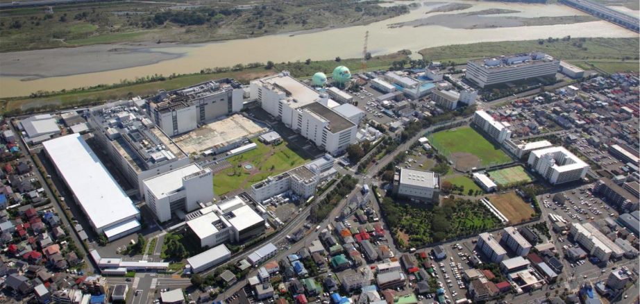
The Sony Atsugi Technology Center sits on about 25 acres next to the Sagami River in Kanagawa, Japan. It’s a 1 hour ride southwest of Tokyo. I take the subway to Shinjuku Station. It’s rush hour. Locals call it sushizume, like sushi in a bento box, also described as 198% congested, which means “can barely read a folded newspaper.” No wonder everyone is reading on smartphones.
Yutaka Okahashi has kindly offered to meet me at Shinjuku. Otherwise I would never have found the required Romancecar of the Odakyu Electric Railway. It’s reserved seating, an oasis of calm, and named “Romancecar” because of the double seats that don’t have armrests to separate passengers. The train services the resorts of Hakone, a gateway to Mt. Fuji, Gotemba and the beach resorts of Odawara and Enoshima. Romancecar trains started running in 1957. They had the world speed record of 90 mph.
The Sony Atsugi Technology Center opened a few years later, in 1960. This is where Sony Atsugi engineers devised Electronic News Gathering (ENG) in 1971. The single operator video camera was developed in 1982, replacing traditional 3-person news crews. The digital VTR was launched here in 1987. In 1989, Atsugi developed SDI. Standard Definition was replaced by many iterations of HD equipment from the mid 80s to 90s. Non-linear digital came in 2000.
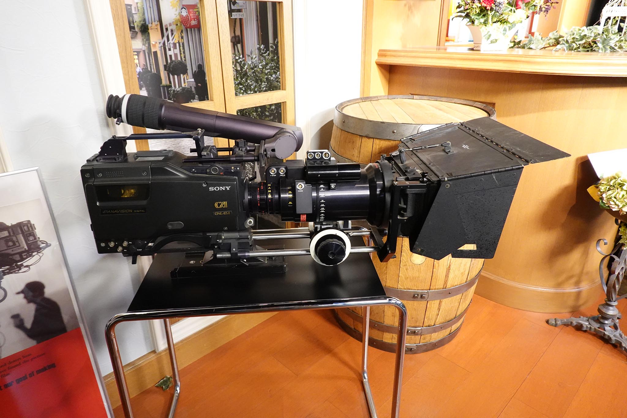
Cinealta digital cine cameras were born at Atsugi in 2000 with the HDW-F900 (HDCAM tape, 24p, three-chip, ⅔˝ CCDs). It was used by George Lucas on Star Wars Episode II. The CineAlta logo was designed in the same year by Hiroki Oka, Chief Art Director at Atsugi. F35 was Sony’s first Super35mm, PL-mount, single-CCD Cinealta camera came in 2008. Next came a rapid succession of digital cine cameras: F3 (CMOS, Super35, FZ mount, SxS cards) in 2010; F65 (S35, PL mount, SRMemory) in 2011; F5 and F55 (S35, FZ mount, SxS and AXSM) in 2012.
And then came VENICE, the camera that came in 2017. That’s the reason we’re here in Atsugi: to visit the team that developed, and continues to support, the Sony VENICE camera.
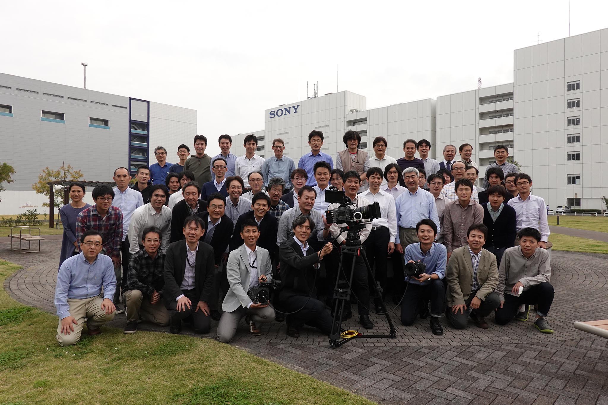
Members of the Atsugi team who designed Sony VENICE. The cameras are manufactured at the Sony Kosai factory, 235 km further southwest.
-

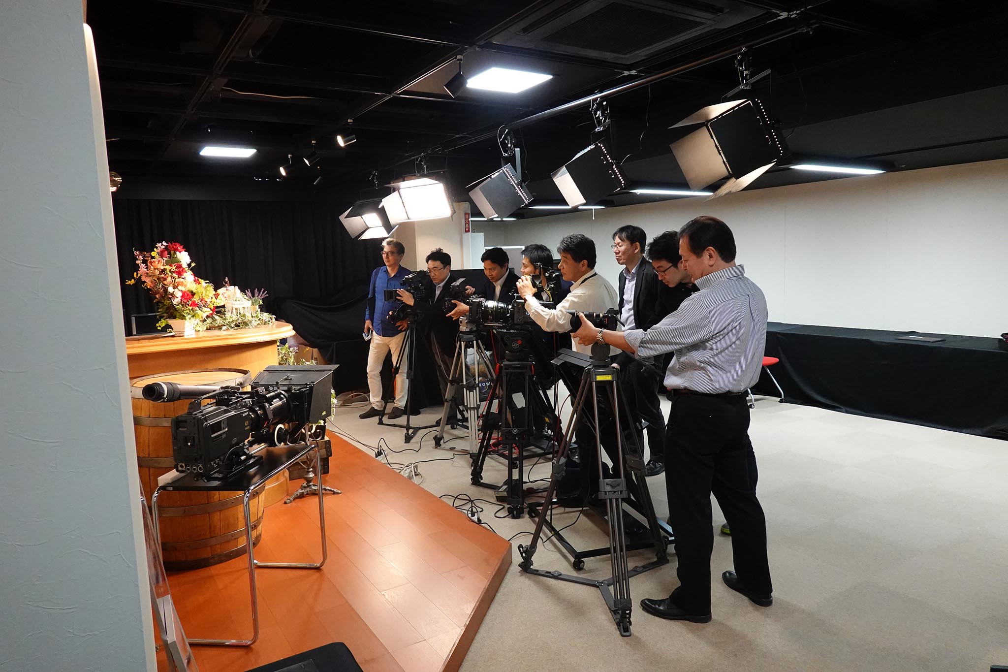
- The studio in Atsugi where cameras are tested.
-
- The Panavised F900 that shot Star Wars Episode II.
-
- Yutaka Okahashi, Product Planner of VENICE, in the studio.
-
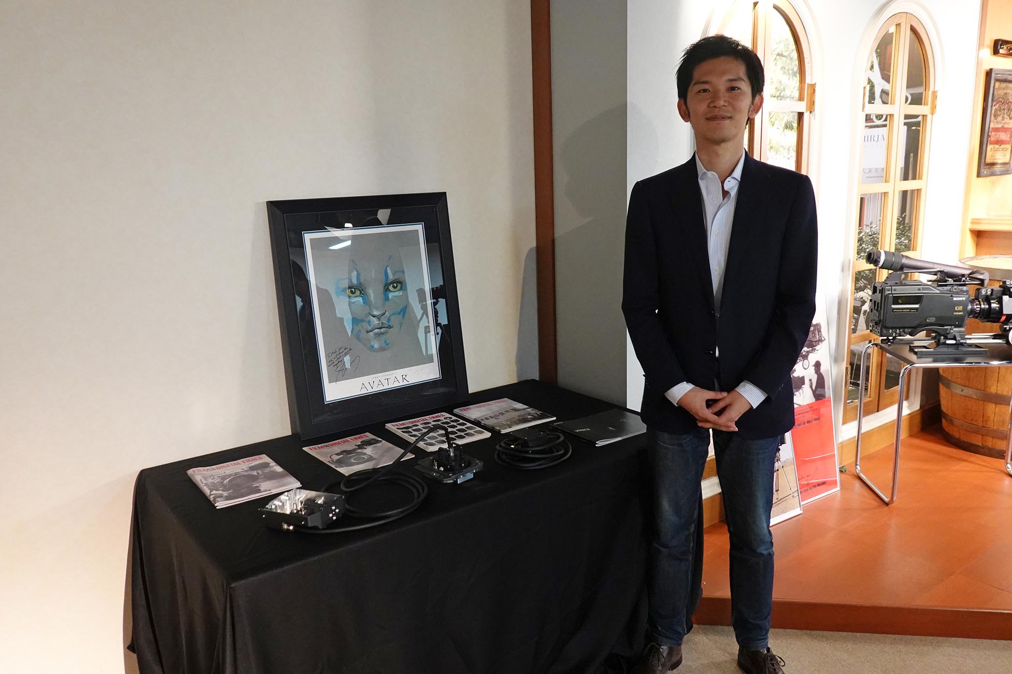
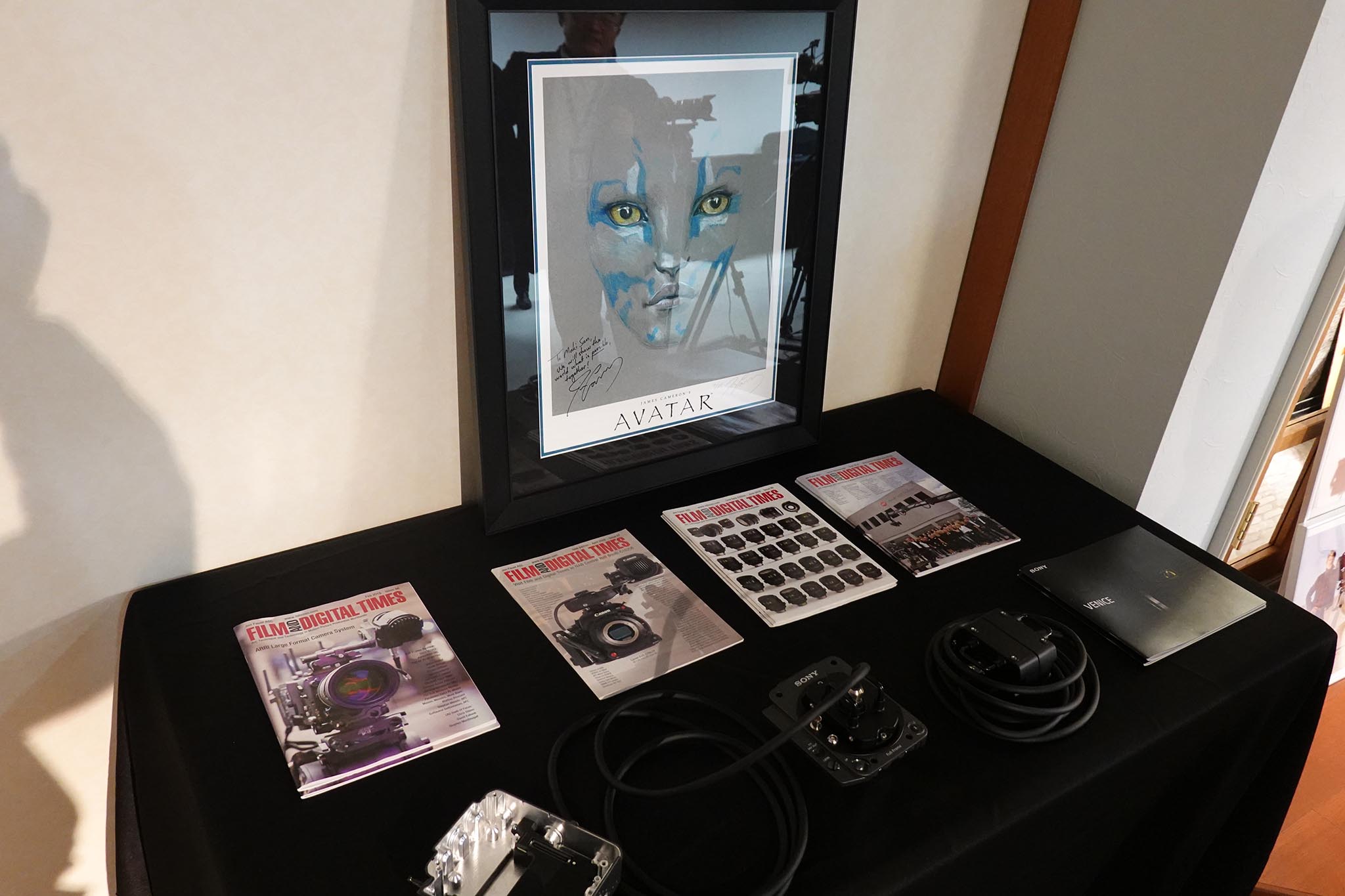
- FDTimes in the studio and Avatar poster. Avatar was shot with Sony F23.
-
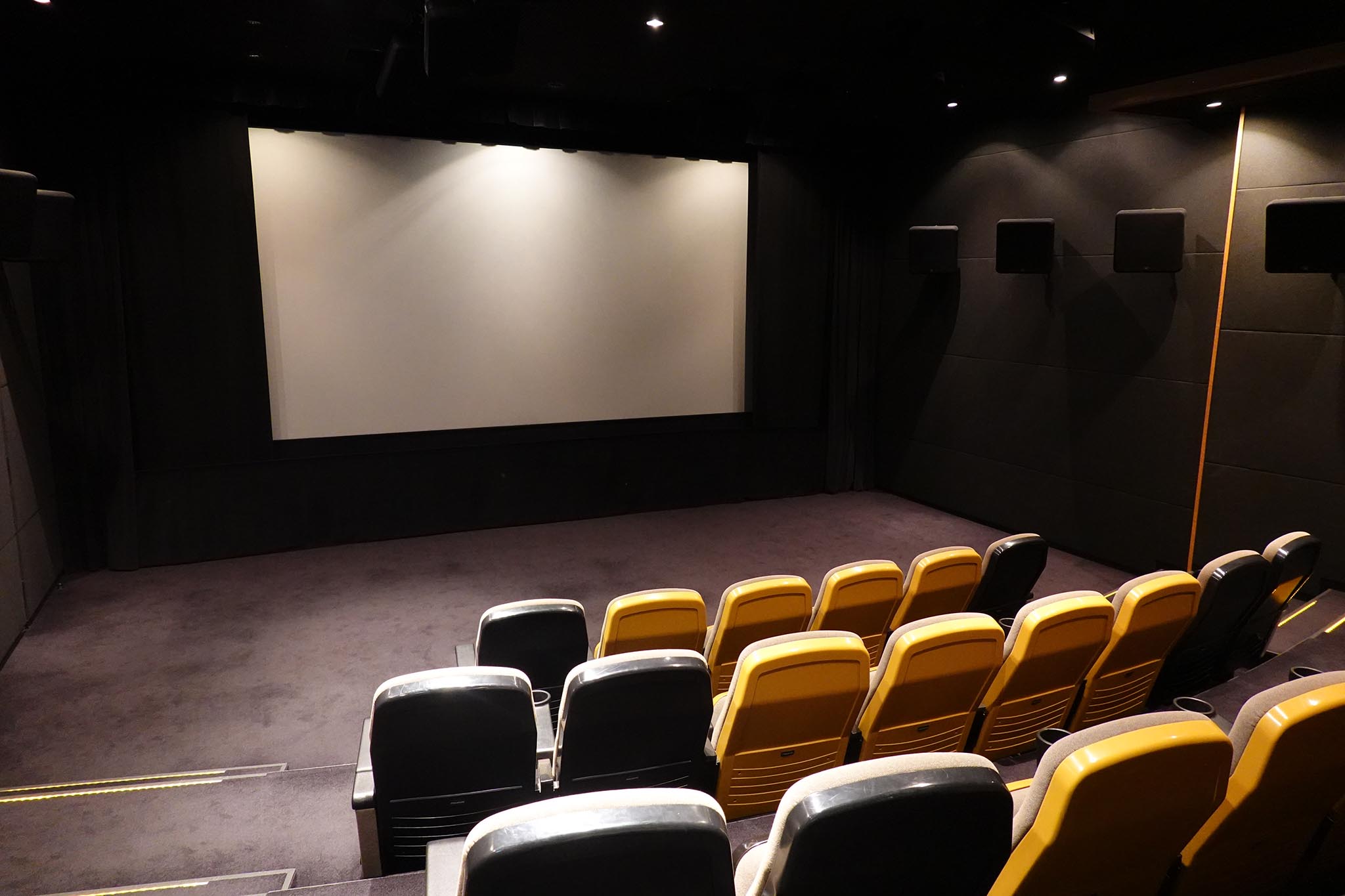
- Sony Digital Cinema 4K Theater in Atsugi.
-
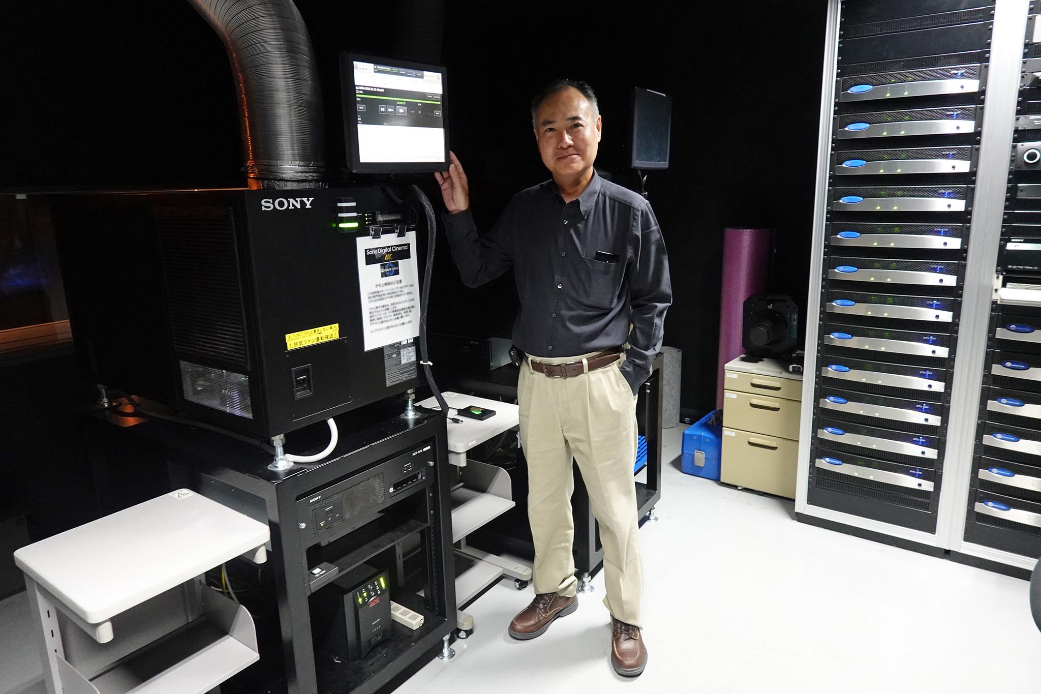
- With Masato Aizawa in the projection room.
-
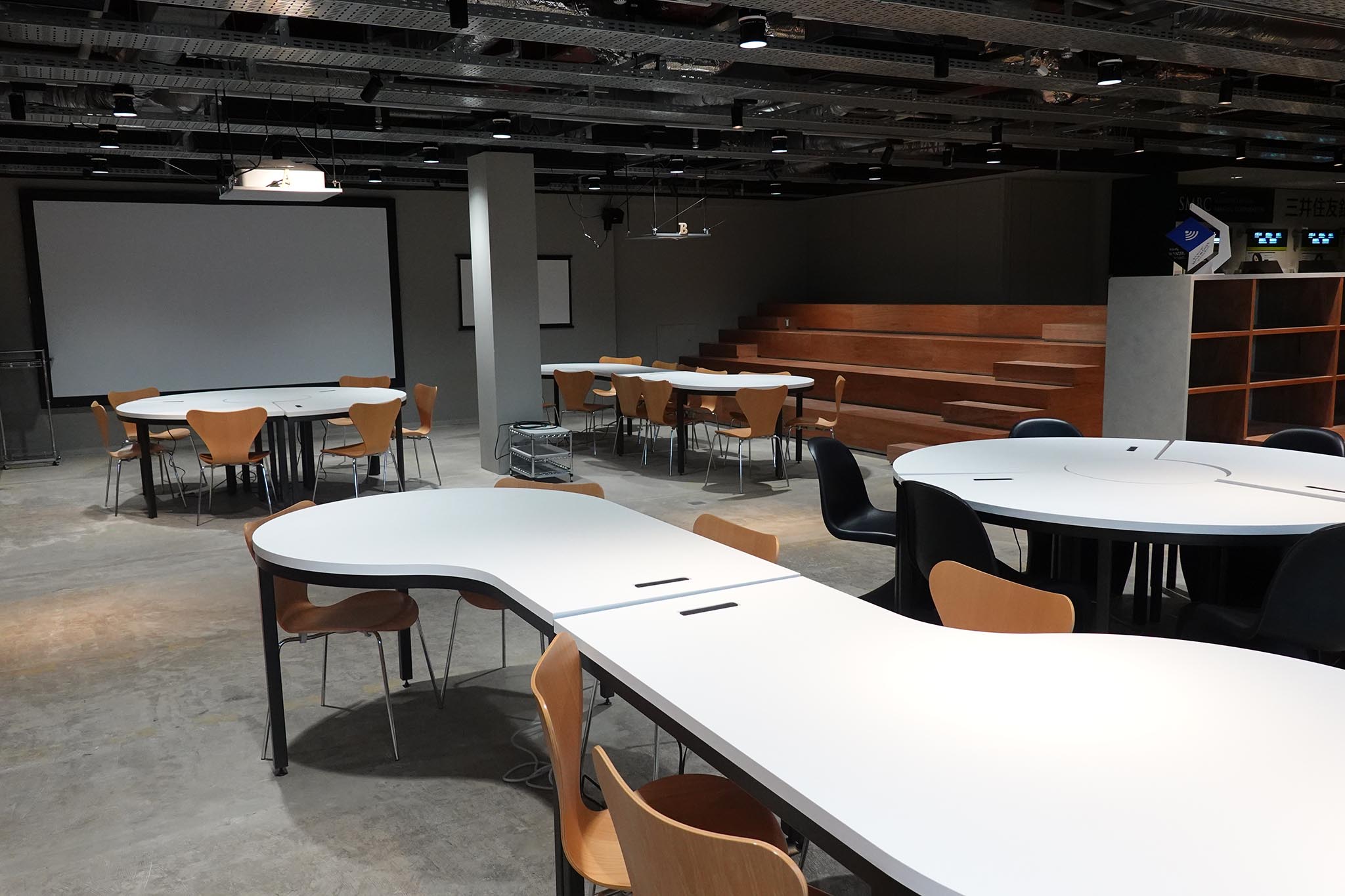
- Atsugi creative collaboration space.
-
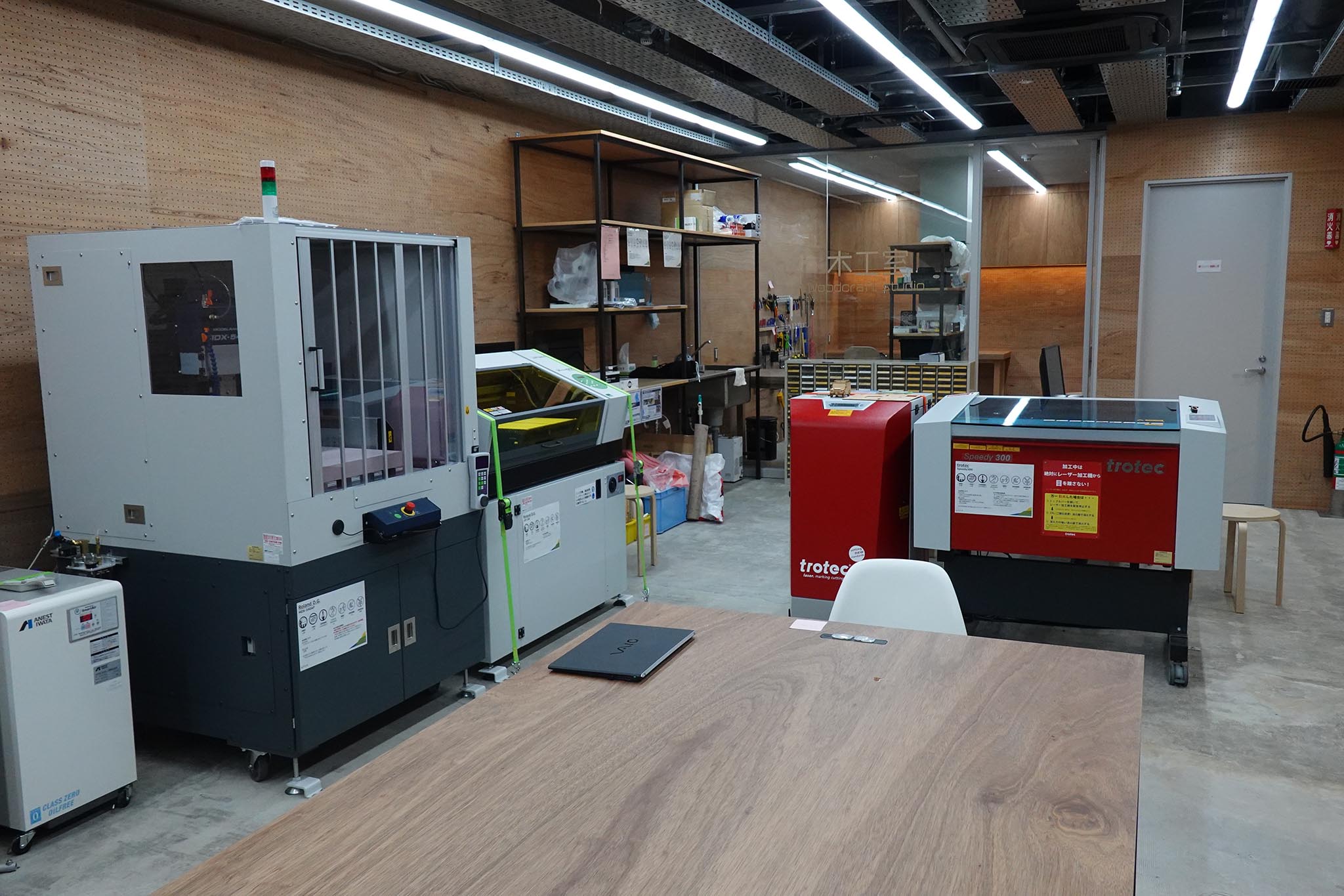
- Creative Space workshop with 3D printers, laser cutters, high tech tools.
-
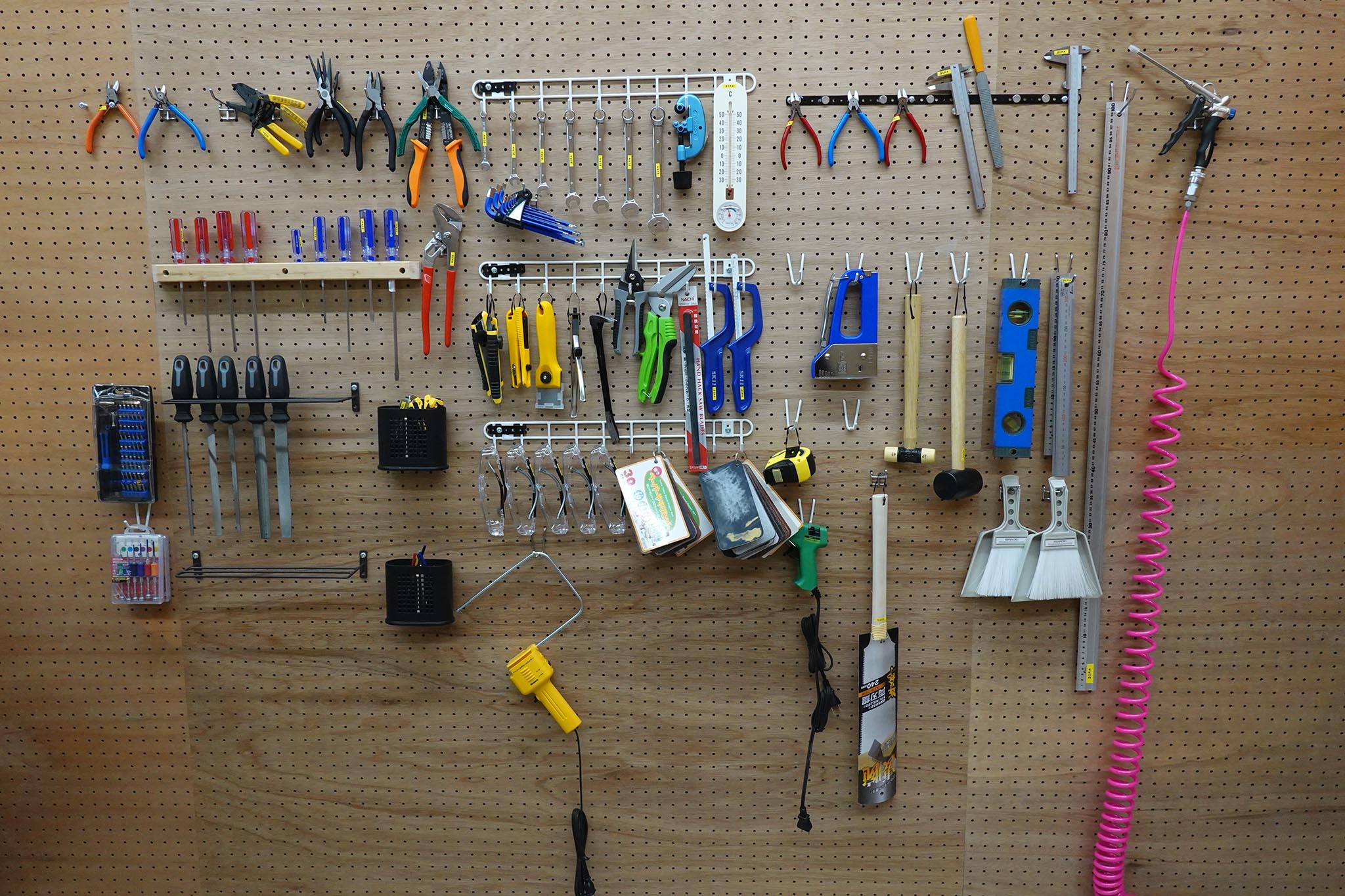
- 24 Pegboard paradise.
-
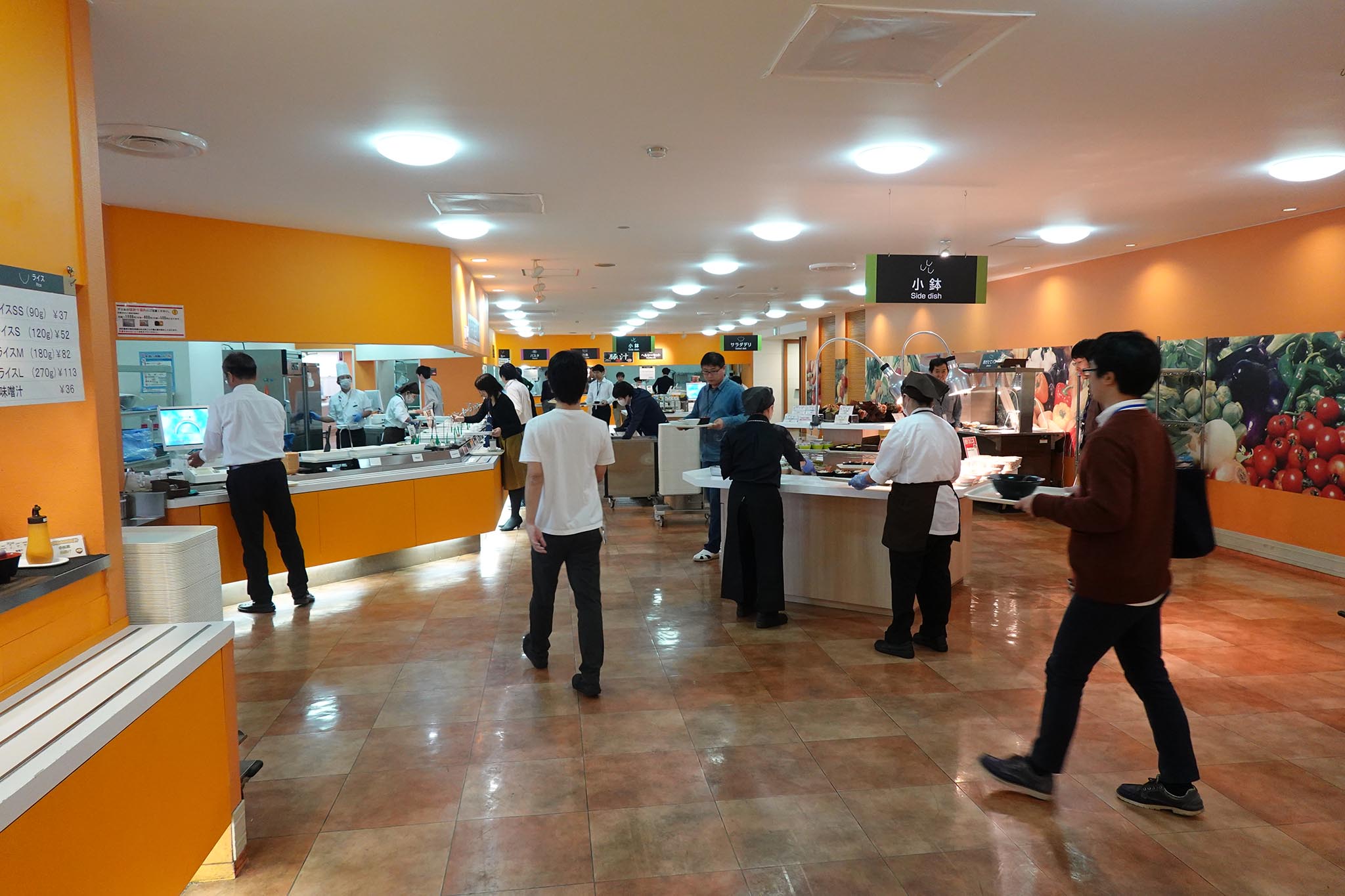
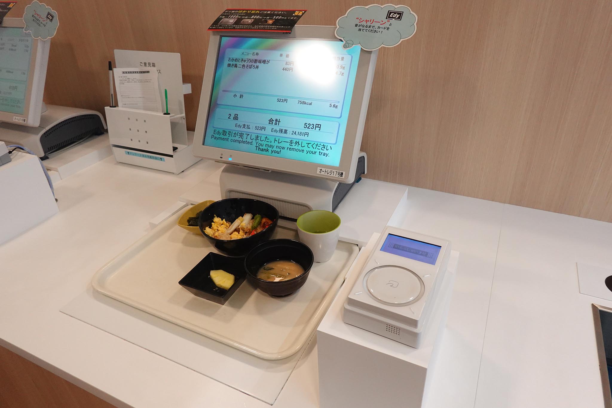
- Lunch time in the Atsugi Cafeteria.
-
- Food is charged according to electronic chips in the bottom of plates.
-
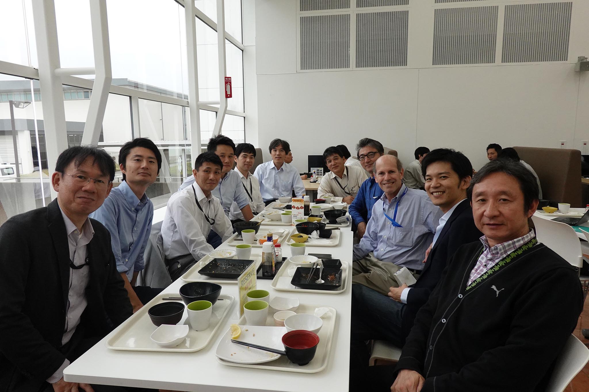
- Lunch with the Atsugi VENICE Team.
Crystal LED Display System
-
- 3200 x 1800 CLED with Toru Suzuki, General Manager of CLED Business Office.
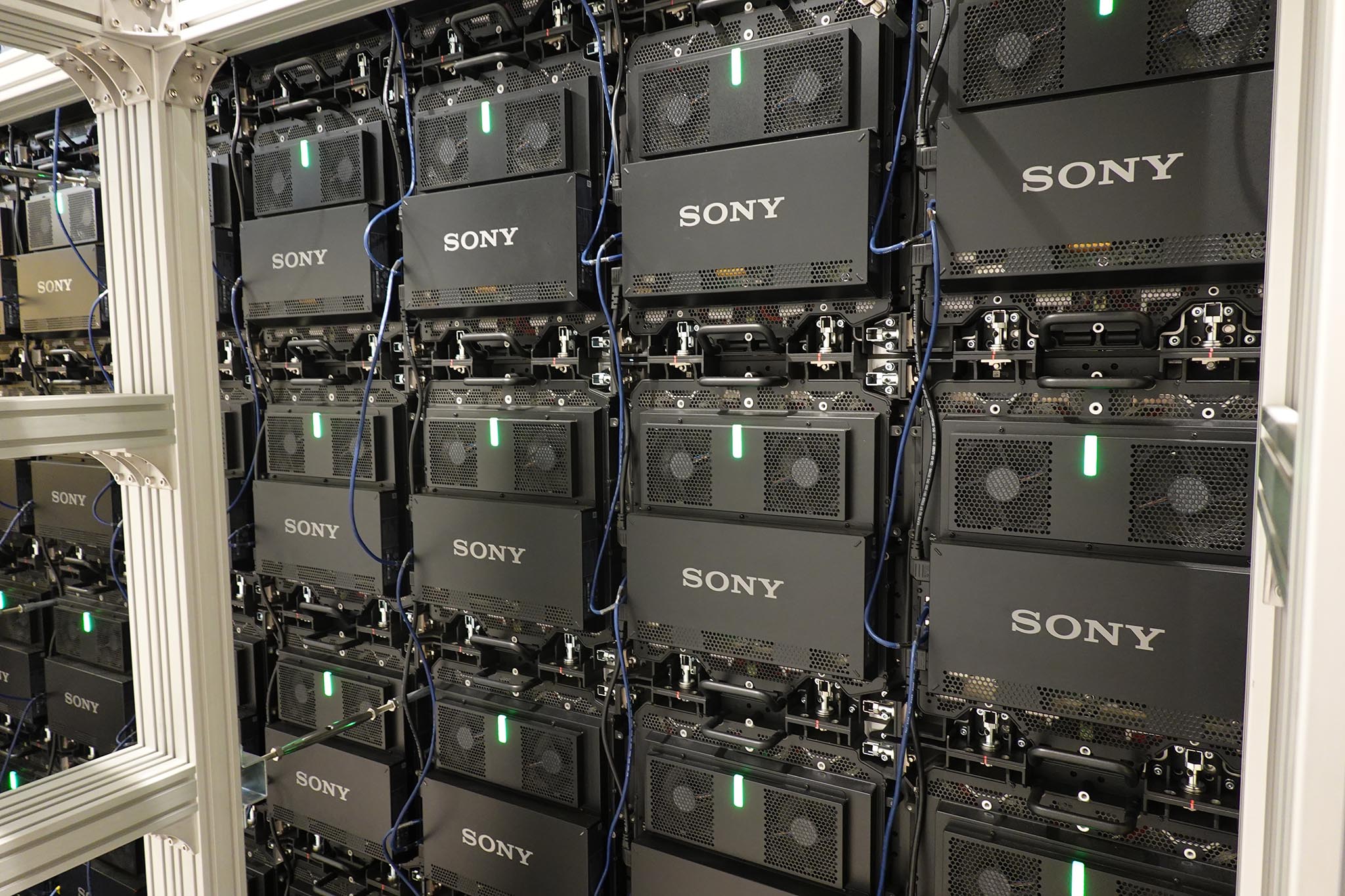
 At the entrance lobby of the Atsugi Technology Center, a large area is devoted to Sony’s Crystal LED (CLED) Display System. They are made up of modular 403 x 453 mm panels that are tiled together to create various sizes. Alignment is achieved with X-Y-Z plots.
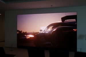
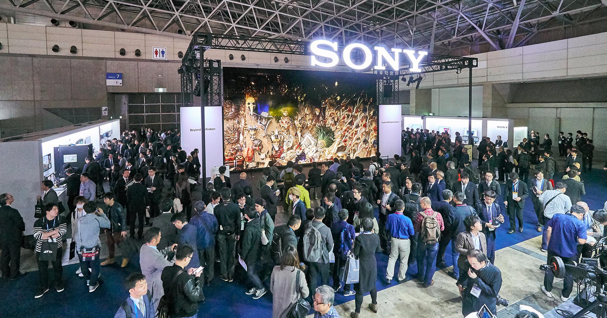
Each microLED pixel is only 0.003 mm2 in size, measuring about half the thickness of a human hair. The display system is 10-bit HDR and 120 fps. Brightness goes up to 1,000 nits and the contrast ratio can be 1,000,000:1. It is scalable in size (and therefore resolution). A huge 8K x 4K Crystal LED wowed the crowds at InterBEE in Chiba in the days that followed (shown below).
Reprinted from Film and Digital Times February 2019 Edition #92